April 5, 2026 · Code available on GitHub
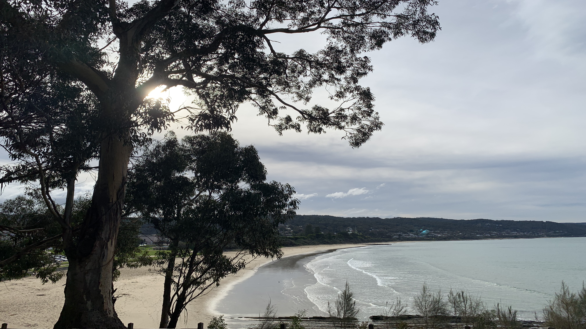
This post outlines a project of mine where I built a JPEG encoder on an FPGA. The image you see above was encoded on my FPGA. This post briefly goes over how JPEG encoding transfers to FPGAs (from a software engineer's perspective :) ). For a great explanation of how JPEG encoding itself works, I'd recommend this article.
The setup: a Lattice CrossLink-NX FPGA connected to a Raspberry Pi over SPI. The Pi sends raw 1920x1080 RGB pixels, the FPGA compresses them through a full JPEG pipeline, and sends back valid JPEG data.
The full encoding pipeline, 10 modules connected via valid/ready handshakes:
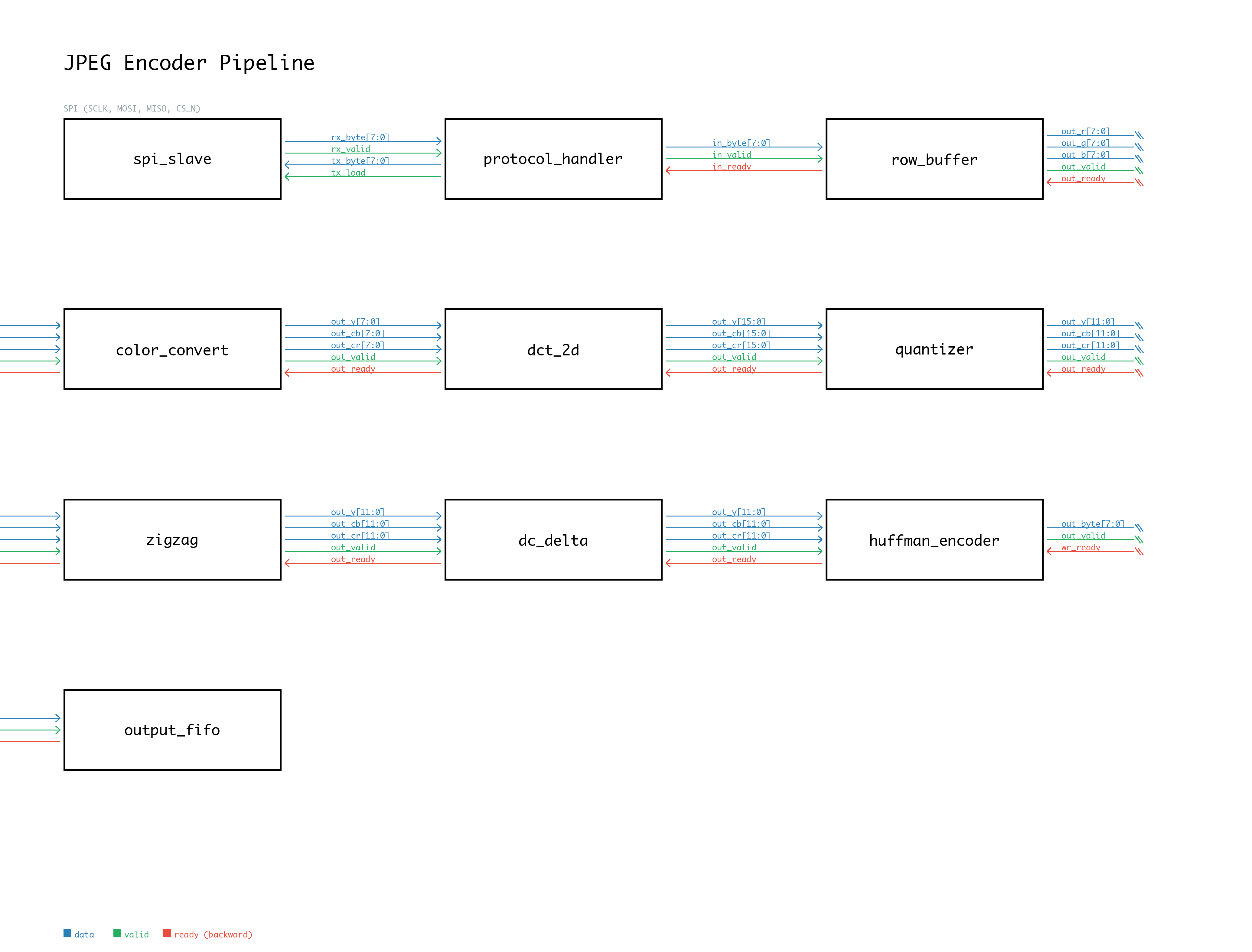
This section runs through the interesting modules from the pipeline.
JPEG operates on 8x8 blocks, but pixels arrive in raster order. In software, you'd just index into a 2D array. On an FPGA, you need to build the memory, decide when to write, and when to read.
The row buffer stores 8 full rows (1920 x 8 = 15,360 pixels) in a dual-port RAM block. A state machine controls the lifecycle:
The hardest part about the DCT on an FPGA: no floating-point unit. Everything has to be fixed-point integer math. Instead of a matrix multiply, we separate the 2D DCT into two 1D DCT passes (rows, then columns). Each 1D DCT is a dot product of 8 values with 8 cosine coefficients.
The DCT needs cosine coefficients like cos(π/16) = 0.9808. On an FPGA there are no floats, so we scale by 1024 and round to get a 12-bit signed integer: round(0.9808 × 1024) = 1004. This is precomputed once and stored in ROM. This is how we multiply 0.9808 × 52 on an FPGA:
All 64 cosine coefficients for the 8×8 DCT are precomputed this way and stored in a single 64-entry ROM of 12-bit signed values. Both the row and column passes use the same ROM since the DCT is separable.
The building block is a multiply-accumulate (MAC) unit: a multiplier feeding into an adder with a 32-bit accumulator register that loops back. Each cycle, one product is added to the running total. With 8 MAC units running simultaneously, all 8 output coefficients for a row are computed at once. Each cycle, one input pixel is broadcast to all 8 MACs, each multiplying by its own ROM coefficient. After 8 cycles the row is done.
The clock waveform below shows the timing: every rising edge, all 8 MACs fire.
Quantization divides each DCT coefficient by a value from a table. Small high-frequency coefficients round to zero. This is where JPEG actually compresses.
Division is expensive in hardware. The trick: multiply by the reciprocal instead. For each table entry Q[i], precompute round(65536 / Q[i]) and store it in a ROM. Then:
quantized = (|coefficient| * reciprocal + 32768) >> 16Huffman encoding produces variable-length codes, so you're no longer working with byte-aligned data.
The encoder maintains a 40-bit shift register as a bit buffer with a 6-bit counter tracking valid bits. Huffman codes (from ROM) and raw coefficient bits are shifted in. When 8+ bits accumulate, a byte is emitted.
The state machine walks through each block's channels sequentially: Y DC, Y AC, Cb DC, Cb AC, Cr DC, Cr AC. For AC coefficients, it tracks runs of zeros for run-length encoding. The bit buffer persists across blocks since the JPEG bitstream is continuous.
Every module implements the same interface: in_valid, in_ready, out_valid, out_ready. A transfer happens when both valid and ready are high on the same clock edge.
A slow downstream module automatically stalls everything upstream. Each module's ready signal is one line of Verilog:
assign in_ready = out_ready || !out_valid;Flow control that would require threads, queues, or async/await in software is just a wire in hardware.
The encoder produces valid JPEG files, pixel-identical to a software encoder using the same pipeline. The image above was encoded entirely on the FPGA.
| Image resolution | 1920 x 1080 |
| Input size | 6.2 MB (raw RGB) |
| Output size | 321 KB (JPEG) |
| Compression ratio | 19.4:1 |
| FPGA clock | ~19 MHz |
| DCT cycles per block | 1,152 |
| Total blocks (1080p) | 32,400 |
AV1...?